Past Experimental Research:
Molecular beam epitaxy of transition metal dichalcogenides
Advised by Prof. Pengpeng Zhang
Molecular beam epitaxy is a technique where solid ultra-pure sources are heated, producing atomic beams which travel through UHV to a heated substrate where the atoms diffuse and incorporate. The samples are grown in a UHV environment which allows for minimal sample contamination and atomically sharp interfaces. By using low growth rates, deposition can be controlled to the sub-monolayer level(i.e. incomplete substrate coverage of a 1 unit cell thickness film).
I have worked on growth of WSe2 and SnSe2 monolayer films on highly-ordered pyrolytic graphite (HOPG). These materials possess electrical properties which could allow heterostructures of them to be used for electronic devices such as tunneling field effect transistors (Appl. Phys. Lett. 108, 2016). The MBE growth of these materials uses elemental sources of W, Se, and Sn and requires careful control of essential growth parameters such as substrate temperature and incident beam fluxes of the elemental sources. To check the growth and ensure that the correct crystal structures were obtained, we used scanning tunneling microscopy which allows atomic resolution images by using the quantum tunneling principle.
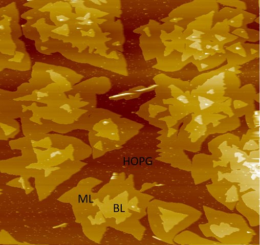
Monolayer (ML) and bilayer (BL) WSe2 on HOPG, 400nm STM scan
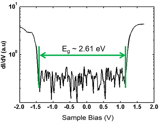
In order to verify the electronic properties of our MBE-grown WSe2, our group has performed scanning tunneling spectroscopy (STS) which allows to probe the density of states. I contributed to this aspect of the research by writing Matlab code to allow automatic analysis of many STS spectra in order to efficiently fit the data and calculate the measured bandgap by averaging over all of the individual fits. Our results showed a measured bandgap of 2.61eV, consistent with literature (Liu et. al. Nature Comms. 6, 2015). Our results are shown below.